1. Full Custom Design Flow
A full custom design flow starts a level lower than that required for semi-custom with the creation of a library of cells. These can then be combined together to build up the complete design. As in a semi-custom process each cell must have a transistor level circuit, an internal mask level layout, a functional model for simulation and an abstract outline for placement and routing. The designer must provide all of these as detailed below.1.1 Cell Design
Cells can be designed in a number of ways. By far the most specialised method is to employ a graphics editor to create and combine a series of polygons. These represent the individual masks that make up the constituent components of the required transistor circuit. A detailed knowledge of mask level geometry is required together with an understanding of process design rules so that correctly defined components can be constructed and manufactured. The following example details a transistor circuit for a CMOS inverter together with its associated mask level layout.
Figure 1.1 Cell Design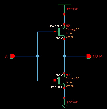
A modern CMOS process can have upwards of a dozen masks to define the complete design. Each will be used to pattern various device elements and their associated interconnect. The main masks required are detailed in the layout above and are listed and described below.
| MASK | DESCRIPTION |
|---|---|
| Nwell | An area of the p-type substrate that will be diffused with n-type impurity to construct the pmos device. |
| Active Area | The areas in the nwell and substrate where the pmos and nmos transistors respectively will be patterned. |
| P Diffusion | The p-type diffusion for the pmos device. Also a ground connection from the gndvss power rail to the substrate. |
| Polysilicon | The transistor channels. Whenever polysilicon crosses an active area a transistor is formed, with source and drain areas either side of the channel and the polysilicon forming the gate connections. |
| Metal 1 | The lower level metal interconnect. |
| Metal 2 | The upper level metal interconnect. |
| Contact | Metal 1 to diffusion/polysilicon connection. |
| Via | Metal 1 to metal 2 connection. |
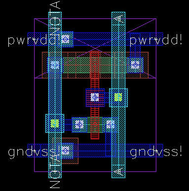
An alternative method of defining the cell layout information is to use a Layout Synthesiser. Here the mask data is now automatically generated from the circuit schematic. The Cadence design system provides this facility. Typically in a full custom topology, cells will be arranged in rows. If all cells have the same height but variable widths they can be horizontally butted and power supply rails can then be tracked straight along the rows. In order to accomplish this a layout synthesiser can compact the cells to a predetermined height. This is also more area efficient. The diagram below shows a layout for the CMOS inverter circuit generated and compacted by a layout synthesiser.
Figure 1.2 CMOS Inverter Circuit
1.2 Cell Verification
In order to verify correct functionality for each cell a circuit simulator such as SPICE/Spectre will be employed. The designer will be required to specify appropriate signal and power supply sources to test the cell in all its operating modes. The following diagrams illustrate a test circuit for the CMOS inverter together with obtained simulation results.Figure 1.3 Cell Verification
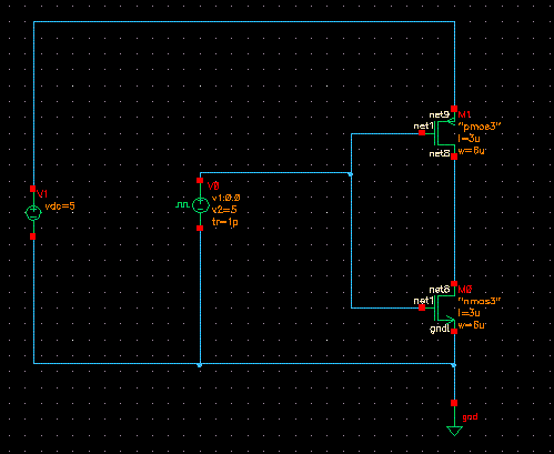
The simulation results enable two important characteristics to be determined for use by the logic simulator.
1) The functionality of the cell. This will be used to define an appropriate logic expression in the functional model.
2) The switching times of the cell measured on the edges of the output waveform. These will be used to define the rise and fall times in the functional model.
1.3 Cell Functional Model
When cells are combined to form the complete design it becomes impractical to simulate this at the circuit level. Simulators such as SPICE cannot handle the resulting complexity and will fail to produce a result. If the design is digital we can construct a functional model for each cell and utilise a gate level logic simulator, such as Verilog, to simulate the assembled design. This is exactly what happens in a semi-custom process except that these functional models have already been provided by the silicon foundry designers. The following text details a typical Verilog functional model for the CMOS inverter.`timescale 1ps / 1ps
`define min_typ_max (0.26:0.5:1.34)
module inverter (A, NOTA);
output NOTA;
input A;
specify
(A*>NOTA) = (`min_typ_max*1600, `min_typ_max*1700);
endspecify
assign NOTA = !A;
endmodule
The `timescale statement defines the time units to be picoseconds.
The `define statement defines a variable array min_typ_max representing scaling factors to be applied to rise and fall times for minimum, typical and maximum operating conditions.
The specify statement defines rise and fall times from input A to output NOTA (1600ps and 1700ps respectively) and computes the overall values for minimum, typical and maximum operating conditions.
The assign statement provides the required logic expression ( ! indicating the invert function).
1.4 Cell Abstract
The cell abstract is generated from the cell layout. It consists only of a cell outline with contact points for the power supply connections and the cell inputs and outputs.Figure 1.4 Cell Abstract

Here we see the cell abstract representing the CMOS inverter layout.
The abstract has been automatically dimensioned to match the height of the other cells in the design.
Contact points for the power and ground rails (pwrvdd! and gndvss! respectively) have been assigned at the top and bottom of the cell. This allows continuous routing along a cell row.
Contact points for the input and output signals (A and NOTA respectively) have been assigned both on the top and bottom edges of the cell. This allows the router to make input and output connections from routing channels either above or below the cell, whichever is the most convenient.
1.5 Design Layout and Verification
The layout strategy employed depends on whether the design is completely full custom or largely standard cell with some full custom components.In a full custom design flow we will need to utilise a layout editor to manually place and route the cell abstracts in an appropriate topology. Typically this will comprise a number of cell rows separated by routing channels. Cells will be placed along the rows and the interconnect tracked along the routing channels. During this process two types of error can be introduced. The first is a violation of the process design rules, for example placing metal tracks too close together. These errors are identified by running the design through a Design Rule Checker (DRC) which can highlight any violations on the layout. The second is an incorrect connection of cells. These are identified by running the design through a Layout Versus Schematic (LVS) checker. This compares the connectivity of components on the schematic with those on the layout and lists any differences.
In a standard cell design flow we can choose a manual or automatic layout or a mix of both. An entirely automatic layout would treat the full custom cells the same as the standard cells and place and route in the normal way. If required we can place and route the full custom cells separately (as is also possible for any standard cell requiring special treatment) and then complete the layout automatically. Alternatively the entire layout can be implemented manually but this is not common. If there has been any manual intervention in the layout process it is essential that both a DRC and LVS are performed to check for errors.
3.3 Complex Gates A library of full custom cells will always comprise the basic primitive functions NOT, AND, NAND, OR and NOR. Additionally there will also need to be some more complex functions such as AND/OR, OR/AND, Multiplexor, Comparator elements etc. These can be assembled using the primitive cells but a more area/speed efficient implementation is achieved by designing these as Complex Gates.
2.1 Complex Gate Structures
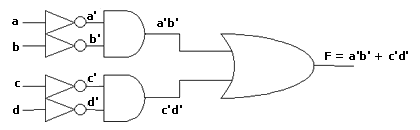
The following examples illustrate a variety of possible implementations for the function F = a' b' + c' d' 1) NMOS Primitive GatesFigure 2.1 Complex Gate Structures
Using standard component library cells in NMOS 5V technology with Zpull-up/Zpull-down > 4/1
Each NOT gate requires 5 transistors (4 x depletion pull-up and 1 x enhancement pull-down).
Each AND gate comprises a NAND gate followed by a NOT gate and requires 15 transistors. The NAND gate needs 10 transistors (8 x depletion pull-up + 2 x enhancement pull-down) and the NOT gate needs 5 transistors again.
The OR gate comprises a NOR gate followed by a NOT gate and requires 11 transistors. The NOR gate needs 6 transistors (4 x depletion pull-up and 2 x enhancement pull-down) and the NOT gate needs 5 transistors again.
The total number of transistors to implement the function is: 4 x NOT gates @ 5 transistors + 2 x AND gates @ 15 transistors + 1 x OR gate @ 11 transistors = 20 + 30 + 11 = 61 transistors.
2.2 CMOS Primitive Gates
Using this technology we can assume that p-type and n-type transistors are of equal size.Each NOT gate requires the area of 2 transistors.
Each AND gate requires the area of 6 transistors (4 for the NAND function and 2 for the NOT function).
The OR gate requires the area of 6 transistors (4 for the NOR function and 2 for the NOT function).
The total number of transistors to implement the function is: 4 x NOT gates @ 2 transistors + 2 x AND gates @ 6 transistors + 1 x OR gate @ 6 transistors = 8 + 12 + 6 = 26 transistors.
2.3 NMOS Complex Gates
Start from the standpoint that any NMOS function has a built-in inversion. So either focus on constructing the inverse function (F') from the outset or accept that a NOT gate will be required to derive the output.Figure 2.3 NMOS Complex Gates

The inverse function is: F' = (a' b' + c' d')'
Using DeMorgan's law F' = (a' b')'. (c' d')'
Using DeMorgan again F' = (a + b) . (c + d)
[DeMorgan's law states that an inverse logic expression can be obtained by inverting each of the terms in the expression and changing all the AND terms to OR and all the OR terms to AND].
Figure 2.4 NMOS Complex Gates

The total number of transistors required = 8 x depletion pull-up and 4 x enhancement pull-down = 12 transistors
It will be considerably faster than the designs based on standard library cells.
2.4 CMOS Complex Gates
One way of constructing a CMOS complex gate is to use the inverse function ( F') to form the pull-down element and the true function (F) to form the pull-up element.Figure 2.5 CMOS Complex Gates

The pull-up section implements the function F = a' b' + c' d'
The pull-down section implements the function F' = (a + b) . (c + d)
Figure 2.6 CMOS Complex Gates

This design would be slightly faster than the one in NMOS.
Summary
A design in NMOS using simple gates drawn from component libraries would require the area taken up by 61 transistors. Using a different technology, CMOS, the same design would be accomplished using 26 transistors. By employing complex gates and NMOS the design can be implemented with 12 transistors and would be considerably faster. Using complex gates and CMOS requires just 8 transistors and the design would be slightly faster again.
3.1 Complex Gate Design
The following methodology is suitable for the design of complex gates.Example - Implement and optimise the following function: Z = [A B + C(A + B)]'
The optimum implementation will involve CMOS.
The equation for the inverse function forming the pull-down section is Z' = [A B + C(A + B)]'
This equation needs to be manipulated to obtain the inverse function for the pull-up section.
Z = (A.B + C(A + B))' by DeMorgan
= (A.B)' . (C(A + B))' by DeMorgan
= (A.B)' . (C' + (A + B)') by DeMorgan
= (A' + B') . (C' + (A'.B') simply expanding the equation
= A'.C' + A'.B' + B'.C' + A'.B' removing the repeated expression
= A'.C' + A'.B' + B'.C'
Z = A'.B' + C'. (A' + B')
Figure 3.1 Complex Gate Design

Note: In this particular example the pull-up section and the pull-down section are identical in structure. This, however, is unusual.
3.2 Complex Gate Optimisation
As we have seen, complex gate structures utilise the lowest number of transistors so are inherently efficient in area and switching speed. Careful design, however, can ensure that these parameters are optimised.Optimised area is obtained by ensuring that the transistor channel widths (W) and lengths (L) are set to the minimum dimension of the fabrication process. These are referred to as Minimum Feature Size devices. For example, in a 0.8 micron process each transistor would have W = L ~ 0.8 micron. This has implications, however, both on the relative switching times and drive capability of the gate. With minimum feature size devices we would expect to have rise times longer than fall times due to the difference in mobility between holes and electrons exhibiting unequal resistance in the p-type and n-type sections. We can compensate for this by increasing the width of the PMOS devices but this takes more area. Likewise with drive strengths. The gate will sink a logic 0 through a lower resistance n-type section better than it will source a logic 1 via a higher resistance p-type section. We can compensate for this with larger PMOS devices but again this requires more area. Typically unless there are specific requirements for equal switching speeds and drive strengths device sizes will be kept to a minimum.
Optimised speed is obtained by:
- Minimising the paths between the gate output and supply rails, Vdd(Power) and Vss (Ground).
- Minimising output capacitance.
- Organising the circuit such that the transistors that are activated later are closest to the gate output.
The first design rule is satisfied, there are only two gates between the output and each rail.
An improvement can be made to satisfy the second design rule. The layout should be organised slightly differently to minimise the number of gates connected to the output and so ensure that the output capacitance is a minimum as shown below.
Figure 3.2 Complex Gate Design

4 Pass Transistor Networks
An alternative approach to the standard logic design techniques so far discussed is to think of a digital circuit as a network of series and parallel switches. In this kind of topology we have some input variables controlling the switches, others as data inputs to the network and transistors utilised as the switches. These transistors are referred to as Pass Transistors since they pass data from input to output. The circuits to be considered utilise n-type devices in an NMOS process.The following truth table defines a pass transistor network for a 2 out of 3 majority function.
ABC F The output is a logic 1 whenever two or more inputs are a logic 1
000 0 The required logic equation is :-
001 0 F = AB + BC + AC
010 0
011 1
100 0
101 1
110 1
111 1
The resulting pass transistor implementation is shown below.
Figure 4.1 Pass Transistor Networks
The variables A and B are used as control variables whilst logic 1, C and logic 0 implement the data lines. Thus when A=B=0 for example the two transistors in the top branch of the network are activated and the input (logic 0) is passed to the output.
The design of pass transistor networks requires a re-arrangement of logic expressions into a more suitable form. Shannon's Theorem provides the required manipulation.
4.1 Shannon's Theorem
The theorem states that any logic expression can be expanded into two terms, the first with a particular variable set to 1, and multiplied by that variable, and the second with it set to 0, and multiplied by the inverse of that variable. By repeating Shannon's theorem with each of the variables involved in the expression, the fullest reduction can be achieved. The method lends itself to automation. It is particularly useful in multiplexor and pass transistor circuit design.Shannon's theorem is stated in a generalised form like this:
A function of many variables, f(a0, a1, a2, ..., ai, ..., an) can be written as the sum of two terms, one with a particular variable (say ai) set to 0, and one with it set to 1.
f(a0, a1, a2, ..., ai, ..., an) = ai' f(a0, a1, a2, ..., 0, ..., an) + ai f(a0, a1, a2, ..., 1, ..., an)
Example
Let's say the function f(a,b,c,d) is defined as f(a,b,c,d) = a b d + a' c
When a is zero, fa=0 = 0 b d + 1 c = c
When a is one, fa=1 = 1 b d + 0 c = bd
Now using Shannon, f(a,b,c,d) = a'fa=0 + afa=1 = a' (c) + a (b d)
Shannon can be generalised for more than one control variable.
Example using two control variables
Starting with the same function f(a,b,c,d) = a b d + a' c
f = a' b' fa=0&b=0 + a' b fa=0&b=1 + a b' fa=1&b=0 + a b fa=1&b=1
= a' b' (c) + a' b (c) + a b' (0) + a b (d)
Example using three control variables
Starting with the same function f(a,b,c,d) = a b d + a' c
f = a' b' c' fa=0&b=0&c=0 + a' b' c fa=0&b=0&c=1 + a' b c' fa=0&b=1&c=0 + a' b c fa=0&b=1&c=1
+ a b' c' fa=1&b=0&c=0 + a b' c fa=1&b=0&c=1 + a b c' fa=1&b=1&c=0 + a b c fa=1&b=1&c=1
= a' b' c' (0) + a' b' c (1) + a' b c' (0) + a' b c (1) + a b' c' (0) + a b' c (0) + a b c' (d) + a b c (d)
4.2 Pass Transistor Design
Shannon's theorem will be applied using n-1 variables as controls and three data lines namely 1, 0 and the remaining nth variable. Let the control signals flow vertically and the data flow horizontally.Place n-type transistors at the intersections to satisfy the expanded Shannon function.
Remove pairs of transistors where they cancel one another out.
Example
f(a,b,c,d) = a b d + a' c
= a' b' c' (0) + a' b' c (1) + a' b c' (0) + a' b c (1) + a b' c' (0) + a b' c (0) + a b c' (d) + a b c (d)
Figure 4.2 Pass Transistor Design
Figure 4.3 Pass Transistor Design
The construction of a pass transistor network must be such that one and only one branch is active at any given time. If more than one branch is active the output can be connected to different logic levels thereby resulting in a corrupted output. Having none of the branches active renders the output of the network high impedance and therefore open circuit to any load it is driving.
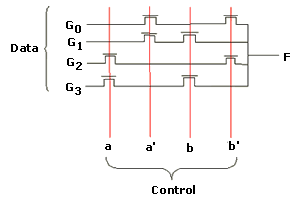
5 Universal Logic Modules
Components that can implement a varied set of logic functions from a single structure are known as Universal Logic Modules (ULM). They are particularly useful in Programmable Logic Device (PLD) architectures where an array of identical logic cells is replicated across the chip with each cell programmable for a range of required functions. Pass transistor networks are ideally suited to these type of applications since they can provide standard structures with variable functionality determined by the choice of control and data variables.Consider the Shannon expansion for a two variable function.
F = f(a,b)
= a' f(0,b) + a f(1,b)
= a' f0 + a f1
So when a=0, F = f0 and when a=1, F = f1.
By setting f0and f1 to different combinations of logic 0, b and logic 1 we can obtain a variety of logic expressions as shown below.
For example, by setting f0 = 0 and f1 = b the logic expression for the output becomes the AND function F = a'.0 + a.b = a.b
Figure 5.1 Universal Logic Modules

F = f(a,b)
= a'b'G0 + a'bG1 + ab'G2 + abG3
This provides a more flexible, programmble implementation as shown below:
Figure 5.2 Universal Logic Modules
Không có nhận xét nào:
Đăng nhận xét